


Sony and TSMC Join Forces to Advance Image Sensor Technology
 9
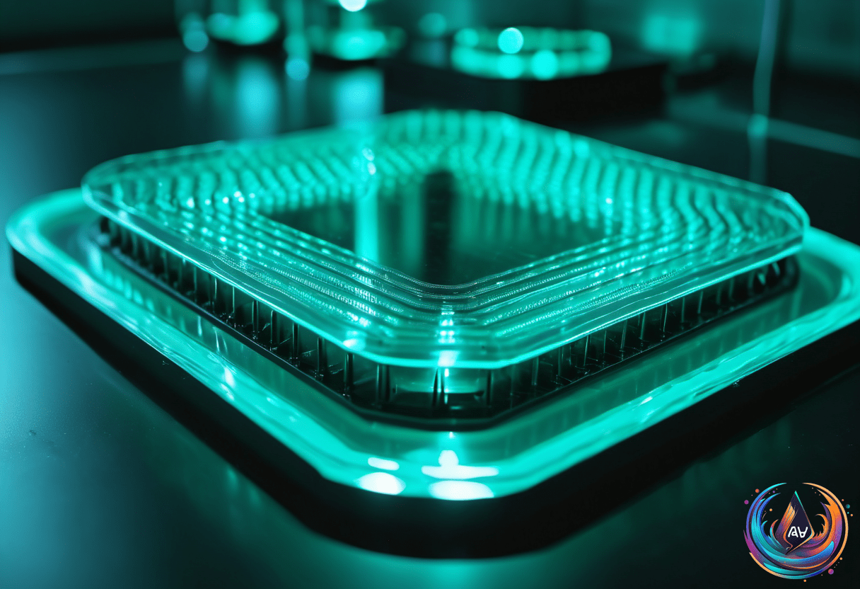
9Sony and TSMC are teaming up to push the boundaries of image sensor technology. They have announced a strategic partnership that aims to combine Sony’s expertise in sensor design with TSMC’s advanced manufacturing processes. The goal is to develop higher-performance sensors for emerging markets like AI, automotive, and robotics.
New Joint Venture in Japan
The two companies plan to establish a joint venture, with Sony holding the majority stake. This venture will set up development and manufacturing facilities at Sony’s new semiconductor plant in Kumamoto, Japan. The partnership is designed to enhance supply capabilities and meet growing global demand for high-quality image sensors.
Sony’s sensor design experience will complement TSMC’s manufacturing prowess. The collaboration aims to create cutting-edge sensors that can handle the demands of AI and automotive industries. Both companies see this as a way to stay competitive and innovate in a fast-changing tech landscape.
Strategic Investment and Growth Plans
Discussions are underway about potential investments in the new venture, including possible further capital infusion from Sony into its Nagasaki plant. These investments will depend on market conditions and support from the Japanese government. The companies also plan to sign a formal agreement to finalize the partnership.
This collaboration is expected to foster new opportunities by combining design and manufacturing strengths. Sony aims to create high-value sensors that push technological boundaries, while TSMC’s process capabilities will help bring these innovations to market efficiently. The joint venture positions both firms to better serve sectors like AI, automotive tech, and robotics, which require advanced sensing solutions.
In addition, TSMC continues to innovate in semiconductor manufacturing. Recently, it expanded automation using Siemens’ AI-driven design systems, aiming to boost productivity and precision. TSMC also introduced its new A13 process node, which offers smaller, more efficient chips compatible with future high-performance applications. These developments highlight TSMC’s focus on staying at the forefront of chip technology to meet future demands.
Overall, the partnership between Sony and TSMC signals a strategic move to lead in next-generation image sensors. Combining design expertise with cutting-edge manufacturing, the joint venture aims to accelerate innovation and supply stability across key sectors worldwide. This collaboration could shape the future of sensing technology for years to come.


What do you think?
It is nice to know your opinion. Leave a comment.