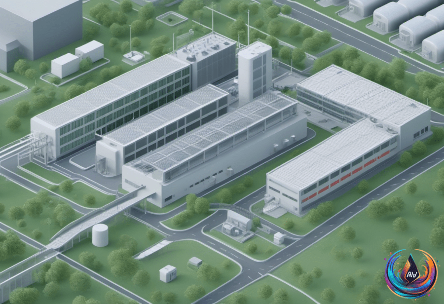
TSMC is doubling down on Taiwan’s semiconductor future. The Taiwanese giant broke ground on three new advanced packaging fabs in the second phase of Chiayi Science Park in southern Taiwan. This expansion targets the industry’s most critical bottleneck: advanced packaging capacity.
The first phase already hosts two fabs that began mass production in June. When both phases operate at full tilt, the park’s output will exceed NT$300 billion ($9.35 billion) annually and sustain roughly 9,000 jobs. TSMC’s market capitalization hovers near $1.96 trillion, and its Q2 revenue smashed records at T$1.27 trillion ($39.62 billion), surging 36% year over year. June alone saw revenue jump 67.9% to T$442.68 billion.
TSMC’s shares have climbed 57% this year. The company offered no updated guidance ahead of its earnings call on Thursday. The Chiayi expansion signals TSMC’s bet on packaging as the key to unlocking higher chip performance.
Across the Pacific, Meta is building a massive 1-gigawatt, AI-optimized data center in Alberta, Canada. The $9 billion project broke ground recently and will be Meta’s first Canadian facility and 33rd worldwide. It promises to employ over 3,000 construction workers at peak and more than 300 operational staff once online.
Meta is also shelling out an extra $40 million for local infrastructure upgrades. The center will deploy a closed-loop, liquid-cooled system paired with dry cooling, a nod to energy efficiency in data center design. Nearby in Louisiana, Meta’s data center campus will be its largest ever—4 million square feet housing over 2 gigawatts of compute capacity.
Optics and AI Speed Breakthroughs
Meanwhile, China’s researchers at Peking University unveiled a new all-optical interconnect system that links standard electronic chips. This innovation boosts AI inference speeds by over 100 times while slashing computational resource needs to one-ninth the norm. Their work, published in National Science Review, uses FPGA chips integrated with a silicon photonic transceiver running at 400 gigabits per second.
Optical interconnects are a growing frontier. Nvidia’s NVLink Fusion, introduced in 2025, blends copper and photonics to let hyperscalers build custom AI systems. Partners include Ayar Labs, Marvell Technologies, and Lightmatter. Nvidia plans to scale from 72 interconnected GPUs today to as many as 576 by 2027. “The physics of copper just changes as you increase the frequency,” said Nvidia’s Jesse Clayton. Transitioning to optics when it fits the platform remains Nvidia’s strategy.
Experts agree co-packaged optics are inevitable. Columbia University’s Keren Bergman said, “More than any other time that I recall, I think it’s concluded that the co-packaged optics will happen.” Ayar Labs’ Vishal Chandrasekar added, “The most optimal way is having a photonic chiplet with an electronic chiplet hybrid bonded.” He expects multiple high-volume photonic implementations by 2028.
China’s PCB Makers Race to Keep Up
China’s printed circuit board (PCB) manufacturers are pouring hundreds of millions into new plants to meet AI-driven demand. Over 20 companies announced aggressive capacity expansions in early 2026. Victory Giant Technology boosted Q1 capital expenditure to 3.6 billion yuan ($530 million), up from 730 million yuan last year. WUS Printed Circuit raised its spending to 1.5 billion yuan from 658 million yuan.
The semiconductor ecosystem is expanding at every link, from chip fabrication and packaging in Taiwan to data centers in Canada and optical breakthroughs in China. The race to power AI is a global sprint, and the stakes couldn’t be higher.
Based on
- TSMC breaks ground on more advanced packaging fabs in Chiayi — thenextweb.com
- Canada’s getting its first Meta data center, and it’s built for AI | Business Insider Africa — africa.businessinsider.com
- Nvlink Fusion Optics Push Past the Copper Wall – IEEE Spectrum — spectrum.ieee.org
- China’s optical chip breakthrough boosts AI speed 100-fold using fraction of compute power | South China Morning Post — scmp.com
- China’s circuit-board makers push capex towards record to feed AI boom | South China Morning Post — scmp.com