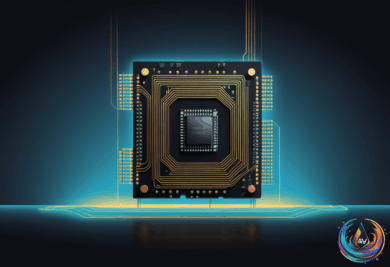
IBM has announced a breakthrough in chip technology. The company created the world’s first sub-1 nanometer chip. This chip uses a transistor architecture at the 0.7 nanometer, or 7 angstrom, node.
This new chip packs nearly 100 billion transistors onto a piece of silicon the size of a fingernail. That is a huge increase in density compared to previous chips. The design uses a new three-dimensional architecture called nanostack. It stacks and staggers transistors vertically in three dimensions, rather than just spreading them out flat.
IBM says this new design offers up to 50% more performance or 70% greater energy efficiency than its 2 nanometer chips. That’s a big jump in power and efficiency. The chip also demonstrates a 40% scaling improvement in SRAM, which is important for faster memory access.
Reinventing Chip Building
Jay Gambetta, director of IBM Research, said, “With our new nanostack architecture, we’re not just making smaller transistors, we’re reinventing how chips are built.” This new approach moves beyond just shrinking sizes. It changes the entire way transistors are arranged and connected.
The nanostack architecture supports logic technology below the 1 nanometer node, venturing into angstrom-scale territory. That means this method could continue scaling chips beyond what was thought possible. IBM’s roadmap projects at least a decade of future scaling using nanostack technology.
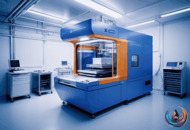
From Lab to Production
IBM developed this technology at its research complex in Albany, New York. The company validated the nanostack design through dielectric bonding in CMOS integration. They even demonstrated a working CMOS inverter based on this technology.
IBM estimates it will take about five years before these nanostack chips enter mass production. The company plans to share more about its commercialization plans later. IBM has a history of licensing semiconductor technologies to companies like Samsung and Rapidus. This new architecture could follow a similar path.
IBM credited partners such as Lam Research, Tokyo Electron, and SCREEN Semiconductor Solutions for helping develop this technology. These companies provide tools and equipment essential for building advanced chips. The role of manufacturers like ASML, known for lithography tools, is also crucial in this process.
This breakthrough comes five years after IBM unveiled its 2 nanometer chip in 2021. The new 0.7 nanometer chip shows that continued progress in shrinking transistor sizes remains possible. It also highlights how innovation in chip design can unlock new performance and energy gains.
The industry leaders like Nvidia’s CEO Jensen Huang, TSMC, and Intel will likely watch IBM’s progress closely. The new nanostack approach could influence the future of semiconductor manufacturing worldwide. For now, IBM has set a new milestone in the race to build smaller, faster, and more efficient chips.
Based on
- IBM says it has created the world’s first sub-1 nanometer chip — engadget.com
- IBM says it has built the first sub-1nm chip technology — thenextweb.com
- IBM Unveils World’s First Sub-1nm Chip Technology, Promises Faster, More Efficient AI Computing | Republic World — republicworld.com
- IBM Debuts World’s First Sub-1 Nanometer Chip Technology — moomoo.com
- IBM Says It Has Found a Way to Keep Shrinking the Technology Inside Chips – DNYUZ — dnyuz.com